Workshop | 9-10 May 2023

Date: 9-10 May 2023
Time: Day 1 from 01.30 - 05.00 pm and Day 2 from 9.00 am - 01.30 pm
ABSTRACT
Scanning Microwave Impedance Microscopy (sMIM) is a near-field scanning probe microscopy technique where an AFM cantilever is used as a microwave source to measure the electrical properties of materials at the nanoscale. sMIM originated at Stanford University and has been commercialized by PrimeNano with the ScanWave product line. In the ScanWave system, microwave signals are sent through a custom AFM cantilever that also collects the reflected signal. The reflected microwave signal is a measure of the impedance of the sample underneath the AFM tip. ScanWave provides images of the variations in the local capacitance and conductance with nanoscale resolution and a sensitivity to capacitance of 0.075 aF. ScanWave is used in the characterization and analysis of a wide range of materials such as semiconductors, insulators, 1D/2D, ferroelectric materials and more.
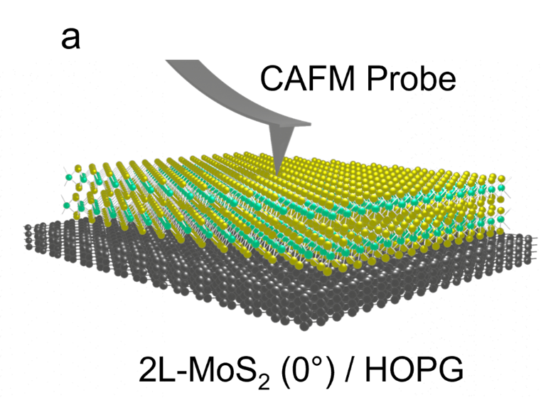
Fig. 1. A schematic of parallel stacked 2L-MoS2 on HOPG (a) is shown
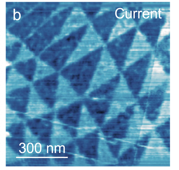
Fig. 1. B: CAFM current map acquired over the bilayer region of the sample
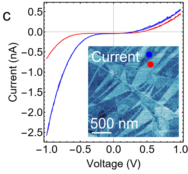
Fig. 1. C: Performing individual current voltage measurements over domains of high and low contrast (c) reveals dramatically different characteristics between domains of each type (inset c).
Image caption
Image caption
James received his PhD in Physics from the University of Nottingham in 2018, studying the morphology and optical properties of monolayers of self-assembled molecules and their heterostructures. He then went on to work as a postdoctoral researcher, also at the University of Nottingham, working on the formation of hybrid heterostructures of molecular assemblies and layered materials demonstrating both electroluminescence and selective triplet excitation. In 2020, James took up a position as a postdoctoral researcher at the Cambridge Graphene Centre, using scanning probe microscopy and optical spectroscopy to study electrostatics and optical properties of layered materials heterostructures with controlled twist angle and their scalable incorporation into integrated photonic circuits. Since January 2022, James has been a member of the Park Systems team as an applications scientist, supporting customers with interest ranging from fundamental physics to industrial scale production in the application of a diverse range of scanning probe microscopy techniques to gain insightful results.