Webinar Series | Fall 2022
Conductive atomic force microscopy (CAFM) uses conductive probes mounted upon a cantilever to measure the current between the probe and a surface with mechanical forces controlled via a feedback loop monitoring the cantilever deflection. CAFM enables both the topography, current maps and current vs voltage characteristics of samples to be measured at nanometre length scales, which yields details of the structure and functional properties of surfaces which cannot be revealed by other techniques. For example: electrical probe stations lack spatial resolution, electron microscopy techniques do not facilitate electrical characterisation and scanning tunnelling microscopy requires surfaces of uninterrupted conductivity. In this webinar, we will review the working principles of CAFM, discuss examples of state-of-the-art measurements and provide a live demonstration of a CAFM experiment.
After introducing the working principles of CAFM, we will explore its applications. We first demonstrate the use of CAFM in exploring the registry of layered materials heterostructures, specifically moiré patterns between single layer graphene and hexagonal boron nitride [1] and reconstructed domains in marginally twisted (0°) 2L-MoS2 [2,3]. After touching on the spatial resolution offered by CAFM, we then discuss its ability to measure localised current vs voltage characteristics in an automated fashion both over individual AB and BA stacked domains in marginally twisted (0°) 2L-MoS2. In the final part of the webinar, we introduce the use of high voltage CAFM to study the breakdown of dielectric layers [4,5] via a live demo and explore its use in extracting the local dielectric strength of materials and studying their breakdown mechanisms.
[1] C. Woods et al. Nature Phys. 10, 451 (2014).
[2] A. Weston et al. Nat. Nanotechnol. 15, 592 (2020).
[3] M. R. Rosenberger et al. ACS Nano 14, 4, 4550 (2020).
[4] Y. Hittori et al. ACS Nano 9, 1, 916 (2015)
[5] A. Ranjan et al. ACS Appl. Electron. Mater. 3, 8, 3547 (2021)
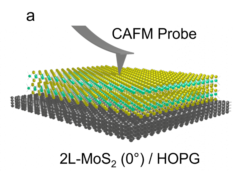
Fig. 1. A schematic of parallel stacked 2L-MoS2 on HOPG (a) is shown
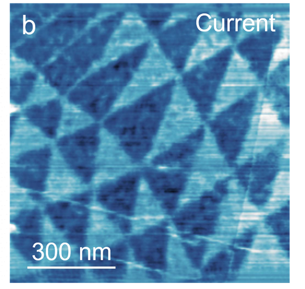
Fig. 1. B: CAFM current map acquired over the bilayer region of the sample
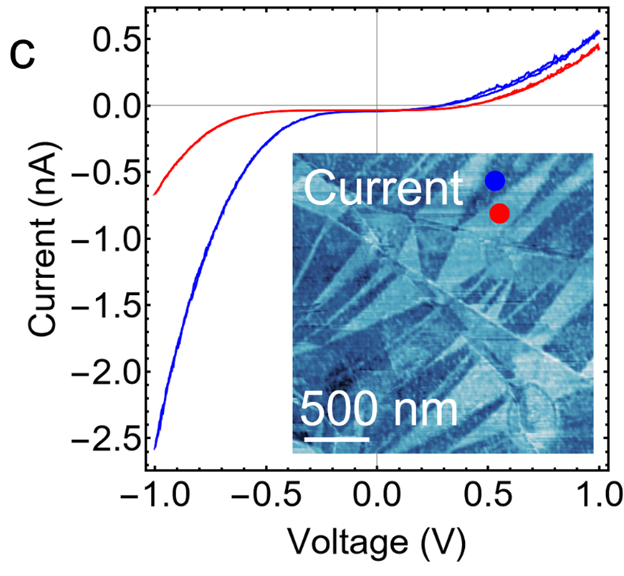
Fig. 1. C: Performing individual current voltage measurements over domains of high and low contrast (c) reveals dramatically different characteristics between domains of each type (inset c).
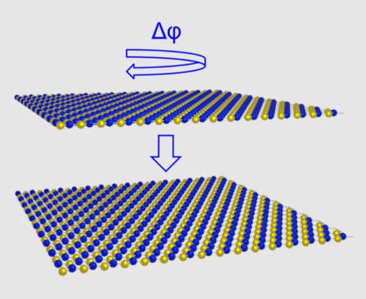
Image caption
Image caption
James received his PhD in Physics from the University of Nottingham in 2018, studying the morphology and optical properties of monolayers of self-assembled molecules and their heterostructures. He then went on to work as a postdoctoral researcher, also at the University of Nottingham, working on the formation of hybrid heterostructures of molecular assemblies and layered materials demonstrating both electroluminescence and selective triplet excitation. In 2020, James took up a position as a postdoctoral researcher at the Cambridge Graphene Centre, using scanning probe microscopy and optical spectroscopy to study electrostatics and optical properties of layered materials heterostructures with controlled twist angle and their scalable incorporation into integrated photonic circuits. Since January 2022, James has been a member of the Park Systems team as an applications scientist, supporting customers with interest ranging from fundamental physics to industrial scale production in the application of a diverse range of scanning probe microscopy techniques to gain insightful results.