


AFM Certification Course
How to Acquire Nanoscale Topography Using AFM
We will again engage in a roughly one-hour lecture applying the finer details of how an AFM operates to the fundamental operational modes (Contact, True Non-Contact™, Tapping, and PinPoint™) used to acquire topography of nanoscale features with a Park Systems AFM. Discussion and questions are welcomed.
Interactive Demo Session Two:
Lecture topics will be reinforced through demonstration and practice of True Non-Contact™, Tapping, and PinPoint™ on a Park Systems NX series AFM. Each imaging mode and sample choice will demonstrate how the AFM is used to gain topographical information at the nanoscale and reinforce operator feedback control of the tip and sample atomic interaction.
Ferroelectricity is observed in hexagonal boron nitride(hBN) through control of the registry of stacked layers, which we explore through both amplitude-modulated and sideband Kelvin probe force microscopy (KPFM) on the Park FX40 automatic AFM.
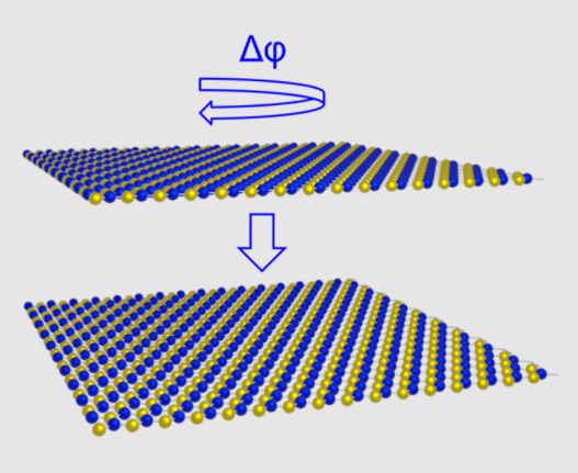
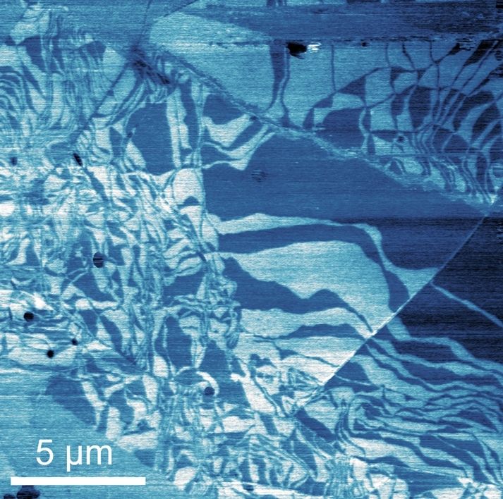
A schematic of the formation of parallel stacked bilayer hBN is shown in addition to a contact potential difference map measured using sideband KPFM.
Image caption
Image caption
Image caption

Ben Schoenek is a Senior Technical Service Engineer for Park Systems, where he focuses on service and support of AFM systems for Park's research user base. He received his Master's in Physics from Auburn University, and holds a B.A. in Physics from Kenyon College.