DHM Webinar Series | 2026
Glass wafers are increasingly adopted as substrates for advanced semiconductor packaging, including glass interposers and TGV-based platforms, where surface waviness, flatness, and roughness are critical for bonding and alignment quality. In this study, Digital Holographic Microscopy (DHM) was applied to characterize the surface topography of a 300 mm bare glass wafer over a large area. Using a 1.25× objective with a 7 × 14 stitching array (98 images, 5.02 µm pixel resolution), full-field height maps were acquired without mechanical Z-scanning and decomposed into waviness and roughness components for quantitative analysis.
Frontside/backside comparison revealed an anti-correlated surface morphology, indicating corrugated deformation through the wafer thickness rather than simple bow or tilt. Local defect features — including bump-like deformations (~90 nm) and crack-like defects (~70 nm depth, ~25 µm width) — were also identified via line profile analysis. These results demonstrate DHM as a practical, non-contact metrology platform for large-area glass wafer inspection with nanometer-scale vertical sensitivity.
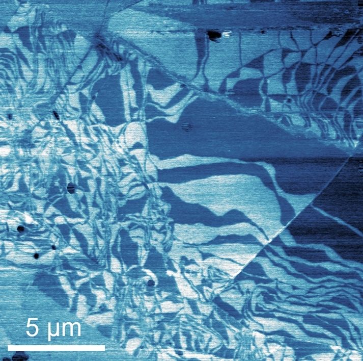
Ferroelectricity is observed in hexagonal boron nitride(hBN) through control of the registry of stacked layers, which we explore through both amplitude-modulated and sideband Kelvin probe force microscopy (KPFM) on the Park FX40 automatic AFM.
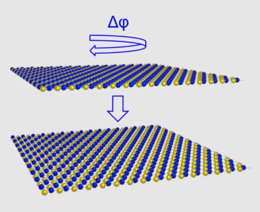
A schematic of the formation of parallel stacked bilayer hBN is shown in addition to a contact potential difference map measured using sideband KPFM.
Image caption
Image caption
Image caption
Ferroelectricity is observed in hexagonal boron nitride(hBN) through control of the registry of stacked layers, which we explore through both amplitude-modulated and sideband Kelvin probe force microscopy (KPFM) on the Park FX40 automatic AFM.
A schematic of the formation of parallel stacked bilayer hBN is shown in addition to a contact potential difference map measured using sideband KPFM.
Image caption
Image caption
Image caption


Chris Jung is a DHM Engineer in the Optical Equipment Division at Park Systems Corporation. He holds a bachelor's degree in Physics with a focus on optics, and completed his graduate research centered on 2D materials.
Before transitioning to optical instrumentation, Chris spent approximately six years as an AFM engineer, building deep expertise in surface metrology and customer-facing technical support. When Park Systems launched its optical equipment division, he joined the team as its dedicated DHM specialist.
With extensive experience across webinars, roadshows, conferences, exhibitions, and customer demonstrations, Chris brings a uniquely broad perspective to applications support, helping customers find practical solutions to their most challenging measurement problems.