
AFM Webinar Series | 2026
This webinar introduces the fundamentals of piezoelectricity and Piezoresponse Force Microscopy (PFM) for researchers who are new to the technique or seeking a practical understanding of nanoscale electromechanical characterization.
The session begins with an overview of the piezoelectric effect, explaining how certain materials generate mechanical deformation in response to an applied electric field. Building on this foundation, the webinar introduces the operating principles of PFM and demonstrates how an atomic force microscope can be used to detect and visualize local electromechanical responses with nanoscale spatial resolution. Key measurement concepts, including PFM amplitude and phase signals, will also be discussed to help participants understand how piezoelectric behavior is interpreted.
The webinar then explores the evolution of PFM techniques, from conventional off-resonance PFM to more advanced methods such as contact-resonance PFM and Dual-Frequency Resonance Tracking PFM (DFRT-PFM). The measurement principles, advantages, and practical applications of each approach will be compared, highlighting how recent developments have improved sensitivity, measurement stability, and quantitative characterization of piezoelectric materials.
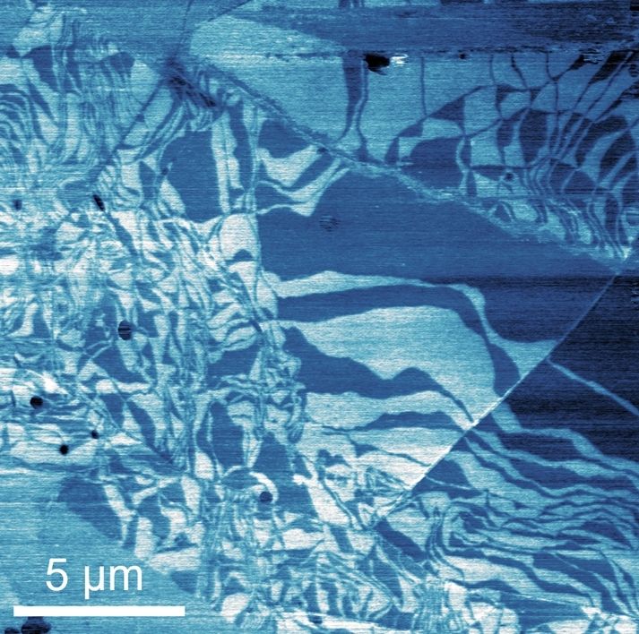
In the final section, recent PFM measurement results from a variety of material systems will be presented to demonstrate the practical capabilities of the technique. Through representative case studies, participants will see how PFM amplitude and phase imaging can be used to investigate local piezoelectric responses, ferroelectric domain structures, domain switching behavior, and nanoscale electromechanical properties across different functional materials. These examples will illustrate how PFM provides valuable insights into material behavior that are difficult to obtain using conventional characterization methods.


Edward Park is a member of the Application Technology Team in the Research Equipment Division at Park Systems. He supports the development and optimization of atomic force microscopy (AFM) applications, with a particular focus on electrical AFM modes and high-resolution nanoscale imaging.With a background in physics and research experience in scanning tunneling microscopy (STM), he applies his expertise to the technical evaluation and advancement of electrical characterization methods and small-area AFM measurements for functional materials and semiconductor devices.