Part of the Electrochemistry Webinar Series.
Go to our Knowledge Center to explore more webinars in this series.
This tutorial webinar introduces the fundamentals of nanoscale electrochemistry, with a focus on Scanning Electrochemical Cell Microscopy (SECCM) implemented on the NX-AFM platform.1 This webinar is designed for researchers who are new to nanoscale electrochemistry as well as those seeking to expand their experimental capabilities using SECCM.
The NX-AFM integrates atomic force microscopy (AFM), nanopipette-based techniques, and top-view (NX10 and NX20) or inverted optical microscopy (NX12), enabling a versatile environment for localized electrochemical measurements. Its core AFM system technology originates from the pioneering invention of AFM at Stanford University in the early 1980s in which Dr. Sang-il Park, CEO of Park Systems was involved.2
SECCM builds on the principles of scanning electrochemical microscopy (SECM), pioneered by Allen J. Bard, and enables the formation of a confined electrochemical cell at the tip of a nanopipette.3 This approach allows researchers to probe electrochemical activity with high spatial resolution, making it particularly useful for studying heterogeneous surfaces, defects, and nanoscale reaction sites.
In this session, we will cover the working principles of SECCM, including nanopipette operation, meniscus formation, and current measurement. Practical guidance on experimental setup, parameter optimization, and data interpretation will be provided. The integration of SECCM with AFM in the NX-AFM platform will also be discussed, highlighting how correlative measurements can link surface topography with electrochemical behavior.
Application examples will include studies of 2D materials,4,5 such as twisted bilayer graphene, and nanocrystal catalysts for CO₂ reduction,6 demonstrating how SECCM can reveal spatial variations in activity and reaction mechanisms.
2. G. Binnig; C. F. Quate; Ch. Gerber; Phys. Rev. Lett. 1986, 56, 930
3. Bard A.J., Fan F.R., Kwak J., Lev O. Anal. Chem. 1989, 1;61(2):132-8.
4. Choi, M.-H.; Noh, H.-A.; Velarde, D.; Yu, Y.; Min, G; and Kaemmer, S.B., Park App. Note #99, 2024
5. Yu, Y., Zhang; K., Parks, H. et al. Nat. Chem., 2022, 14, 267–273.
6. Choi, M.-H.‡; Jeong, S.‡; Jagdale, G.; Zhong Y.; Siepser, N.P.; Wang, Y.; Baker, L.A.*; Ye, X.* J. Am. Chem. Soc. 2022, 144, 28, 12673–12680
Atomic force microscope image of unidirectionally directionally controlled grown nanofibers
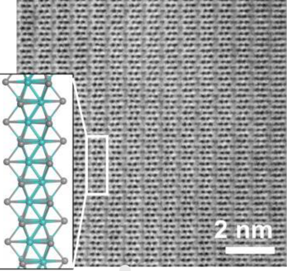
Electron microscope image and structural model of TMC atomic wire nanofibers aggregated in the same direction
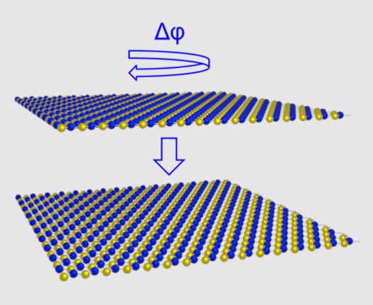
Image caption
Image caption
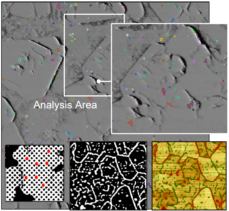
Ferroelectricity is observed in hexagonal boron nitride(hBN) through control of the registry of stacked layers, which we explore through both amplitude-modulated and sideband Kelvin probe force microscopy (KPFM) on the Park FX40 automatic AFM.
A schematic of the formation of parallel stacked bilayer hBN is shown in addition to a contact potential difference map measured using sideband KPFM.
Image caption
Image caption
Image caption

Brian received his Ph.D. in Analytical and Materials Chemistry from Indiana University Bloomington in 2022, where he employed scanning electrochemical cell microscopy (SECCM) to measure single-particle electrocatalytic activity at facet-controlled nanocrystals. He subsequently joined Texas A&M University as a Postdoctoral Research Specialist in Chemistry, where he designed and conducted multidisciplinary research at the intersection of materials science, electrochemistry, and nanomaterial fabrication. His work centered on SECCM for spatially resolved measurements of local electrochemical reactivity at individual nanoparticles and nanocrystal facets. In parallel, he mentored graduate students across a broad range of microscopy platforms, including SEM, FIB-SEM, AFM, SICM, and SECCM.
In March 2023, Brian joined Park Systems as a Senior Applications Scientist, bringing together his multidisciplinary research expertise and prior industry experience gained during his previous role as an Application Engineer and Product Marketing Manager at Park Systems headquarters in South Korea from 2009 to 2017. His current work draws on a broad nanoscale research background, with techniques such as KPFM, conductive AFM, nanomechanical mapping, and photo-induced force microscopy (PiFM) playing central roles in his expanding research activities. Through these approaches, he contributes to a comprehensive understanding of material behavior spanning fundamental surface science to industrial semiconductor applications, while helping researchers and engineers in both academia and industry address complex characterization challenges.