Part of the Electrochemistry Webinar Series 2026

Materials exhibiting mixed ionic–electronic conductivity are central to emerging technologies such as energy storage, bioelectronic interfaces, and neuromorphic computing. In this webinar, I will present advanced techniques to investigate transport processes in these materials under operando conditions using atomic force microscopy (AFM).
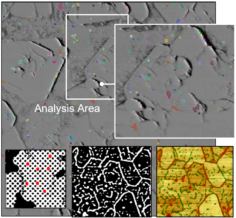
A key phenomenon is the generation of local electrochemical strain resulting from changes in ionic and electronic concentrations within the material. AFM is uniquely suited to detect these small strain amplitudes with high precision, as demonstrated by electrochemical strain microscopy (ESM). I will discuss examples ranging from conducting polymers to battery cathode and anode materials. Furthermore, I will introduce advanced approaches that combine strain measurements with electrochemical impedance spectroscopy to gain deeper insight into transport dynamics. Finally, I will present the concept of strain waves, which enables the investigation of transport processes along mixed-conducting thin films and wires. [1–3]
[2] F. Bonafè, M. Bazzani, B. Fraboni, T. Cramer, Nat. Commun. 2025, 16, 2499.
[3] S. Daboss, T. Cramer, N. Franke, B. Fraboni, C. Kranz, J. Microsc. 2025, 1.
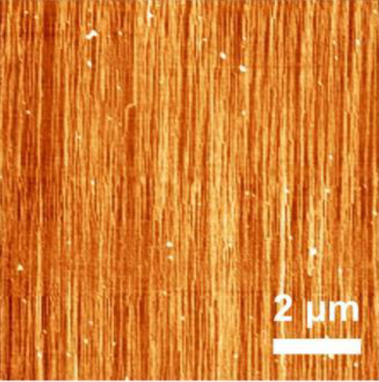
Atomic force microscope image of unidirectionally directionally controlled grown nanofibers
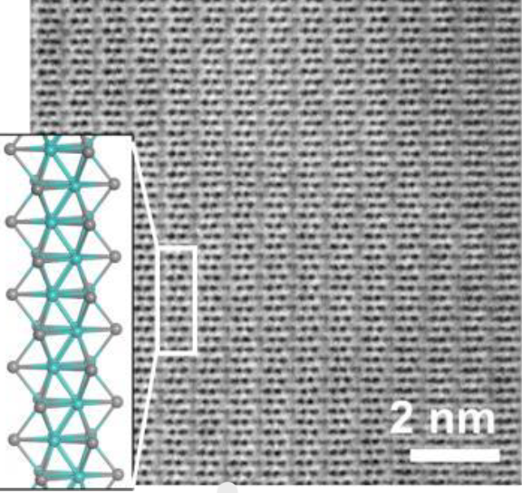
Electron microscope image and structural model of TMC atomic wire nanofibers aggregated in the same direction
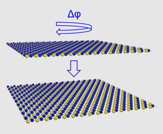
Image caption
Image caption
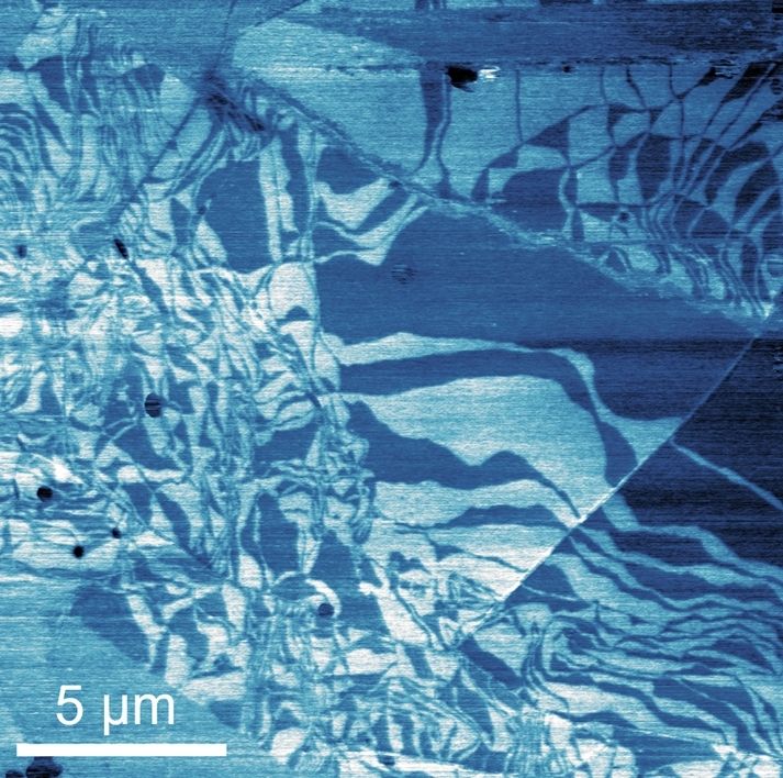
Ferroelectricity is observed in hexagonal boron nitride(hBN) through control of the registry of stacked layers, which we explore through both amplitude-modulated and sideband Kelvin probe force microscopy (KPFM) on the Park FX40 automatic AFM.
A schematic of the formation of parallel stacked bilayer hBN is shown in addition to a contact potential difference map measured using sideband KPFM.
Image caption
Image caption
Image caption


Tobias Cramer is Associate Professor of Condensed Matter Physics at the Department of Physics, University of Bologna. His research focuses on nanostructured and organic electronic materials for sensors and transducer applications, with particular emphasis on charge transport and transduction processes at semiconductor–electrolyte interfaces where ionic and electronic carriers coexist. His group develops macroscopic and microscopic experimental approaches to study how electrical properties are linked to material structure, mechanical deformation, and interfacial phenomena.
In recent years, his work has increasingly addressed organic mixed ionic–electronic conductors, with applications ranging from low-invasive biosensors and electrophysiology to energy conversion and storage systems. His expertise spans flexible and stretchable electronics, atomic force microscopy, implantable and bioelectronic devices, and human–technology interfaces.
Tobias Cramer studied chemistry and physics in Freiburg, Germany, where he obtained his PhD. He subsequently worked in several international research laboratories, including ISMN-CNR (Bologna), The Scripps Research Institute (San Diego), Philips Research (Eindhoven), and the Department of Microsystems Engineering (Freiburg). He has participated in multiple European research projects and has served as principal investigator and work-package leader. Tobias Cramer is author of more than 70 scientific publications and co-organizer of the annual International Winter School on Bioelectronics in Kirchberg, Austria.