Part of the FX200 Webinar Series: Exploring layered materials with automated Atomic Force Microscopy

Ferroelectric materials are of great interest for next-generation electronics as they enable devices with non-volatile memory by changing the orientation of dipoles in the ferroelectric. Such research benefits greatly from techniques that are able to measure and manipulate ferroelectricity over nanometre length scales. Atomic force microscopy (AFM) is the ideal tool to meet this challenge since its possesses functional modes sensitive to electrostatic forces, surface potential and piezoresponse with nanoscale resolution, as well as the ability to manipulate ferroelectrics by using applied bias through the tip.
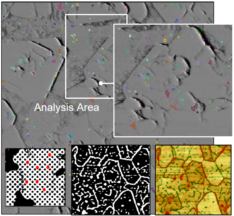
In this webinar, we showcase the unique abilities of our FX series AFMs to measure and manipulate ferroelectricity. Our FX series AFMs are able to automatically change probe and functional mode, which we will demonstrate by performing heterodyne Kelvin probe force microscopy HD-KPFM and dual frequency resonance tracking piezo response force microscopy (DFRT-PFM) to measure ferroelectricity in parallel stacked hBN and CuInP2S6 flakes, switching to the ideal probe for each measurement with no need to touch the system.
Atomic force microscope image of unidirectionally directionally controlled grown nanofibers
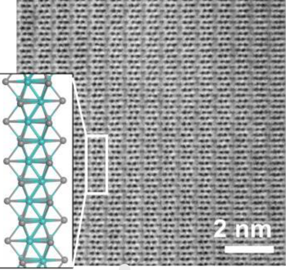
Electron microscope image and structural model of TMC atomic wire nanofibers aggregated in the same direction
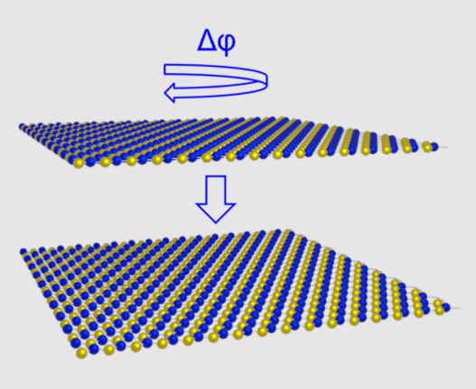
Image caption
Image caption
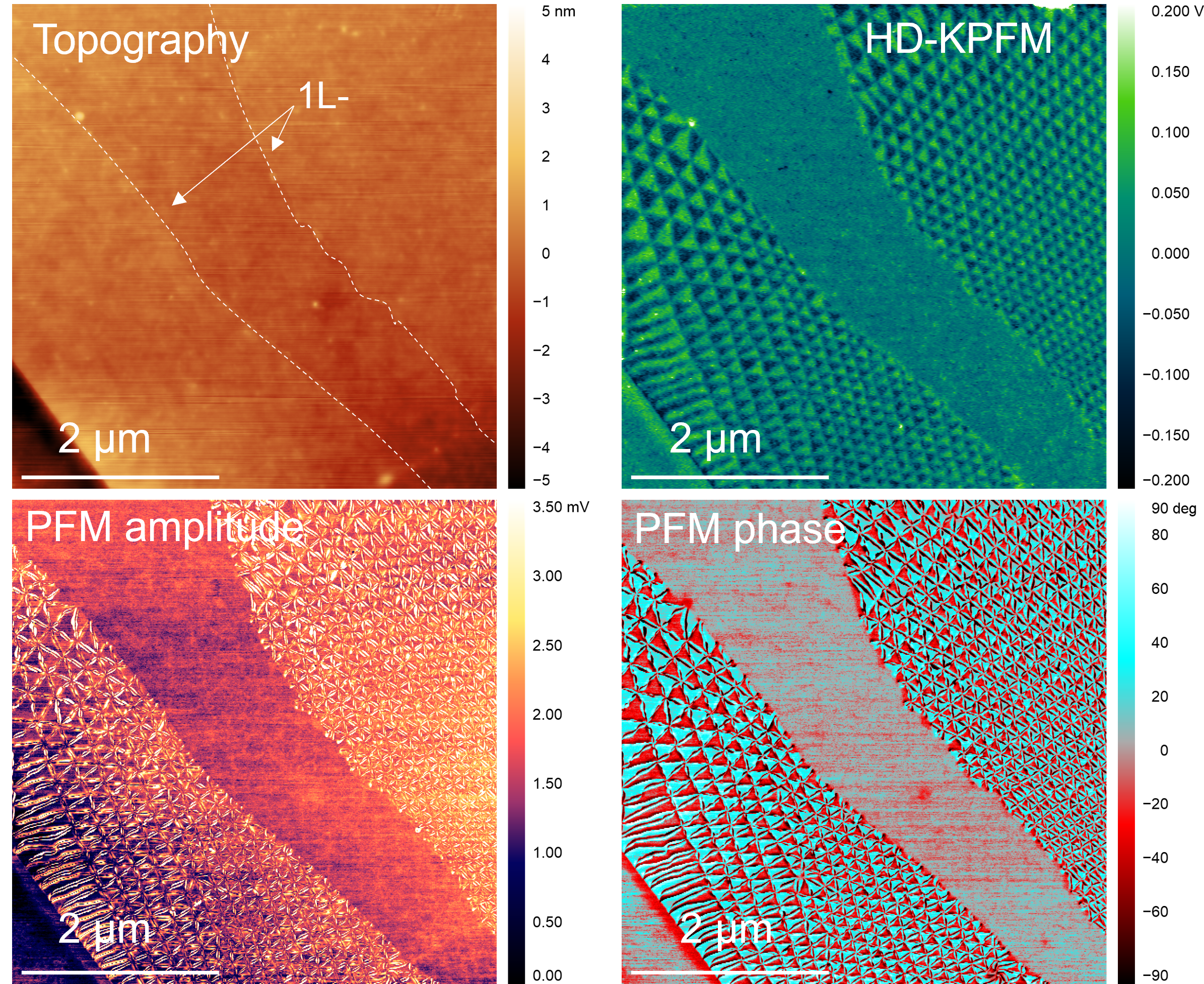
Ferroelectricity is observed in hexagonal boron nitride(hBN) through control of the registry of stacked layers, which we explore through both amplitude-modulated and sideband Kelvin probe force microscopy (KPFM) on the Park FX40 automatic AFM.
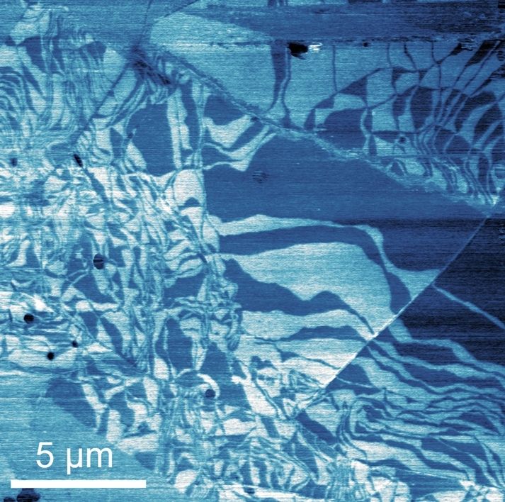
A schematic of the formation of parallel stacked bilayer hBN is shown in addition to a contact potential difference map measured using sideband KPFM.
Image caption
Image caption
Image caption


James received his PhD in Physics from the University of Nottingham in 2018, studying the morphology and optical properties of monolayers of self-assembled molecules and their heterostructures. He then went on to work as a postdoctoral researcher, also at the University of Nottingham, working on the formation of hybrid heterostructures of molecular assemblies and layered materials demonstrating both electroluminescence and selective triplet excitation. In 2020, James took up a position as a postdoctoral researcher at the Cambridge Graphene Centre, using scanning probe microscopy and optical spectroscopy to study electrostatics and optical properties of layered materials heterostructures with controlled twist angle and their scalable incorporation into integrated photonic circuits. From January 2022 to 2024, James was a member of the Park Systems team working as an applications scientist, supporting customers with interest ranging from fundamental physics to industrial scale production in the application of a diverse range of scanning probe microscopy techniques. Following an 18-month postdoctoral position working on tip-enhanced Raman spectroscopy at the University of Nottingham, James rejoined Park Systems in August 2025 working as a technical marketing and applications scientist, showcasing and supporting the implementation of state-of-the-art automated AFM.