Webinar Series | February 2023
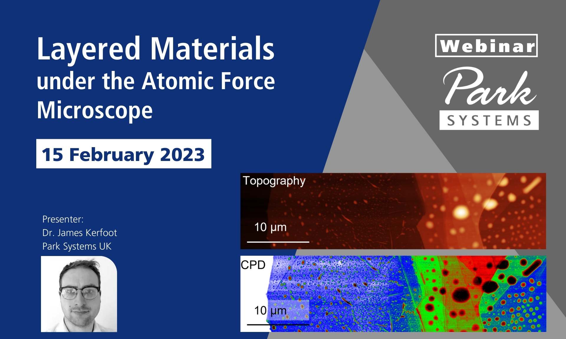
Atomic force microscopy (AFM) is a technique that measures forces between a probe and sample, which can be used not only to measure the topography of surfaces with nanometre scale resolution but to map and manipulate a range of properties which can be addressed via the tip. Here, we touch on but a few of the capabilities of state-of-the-art atomic force microscopy for layered materials research and explore the possibilities to correlate a host of functional properties in one mouse click using our new FX40 automatic AFM.
After introducing the working principles of the measurement of topography, electrostatics and mechanical properties using atomic force microscopy, we will then proceed to perform live nanomechanical [1] and Kelvin probe force microscopy (KPFM) [2,3] measurements on transition metal dichalcogenides which have regions of strain due to trapped interfacial contamination. In addition to studying the interplay of strain and work function in these materials, we will highlight how automated tip exchange enables such measurements to be performed in a less laborious and more reproducible manner.
[1] E. Khestanova. Nat Commun 7, 12587 (2016).
[2] A. Axt, et al. Beilstein J. Nanotechnol. 9, 1809 (2018)
[3] E. Alexeev et al. ACS Nano 14, 9, 11110 (2020)
![]()
Figure 1. (Left) A topography and contact potential difference (CPD) map of MoS2 on silicon measured using KPFM. By estimating the strain from topography measurements over blisters of trapped interfacial contamination, the relationship between strain and work function variation can be extracted for a range of flake thicknesses (right).
Fig. 1. A schematic of parallel stacked 2L-MoS2 on HOPG (a) is shown
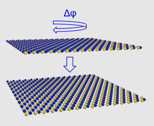


Image caption

Image caption
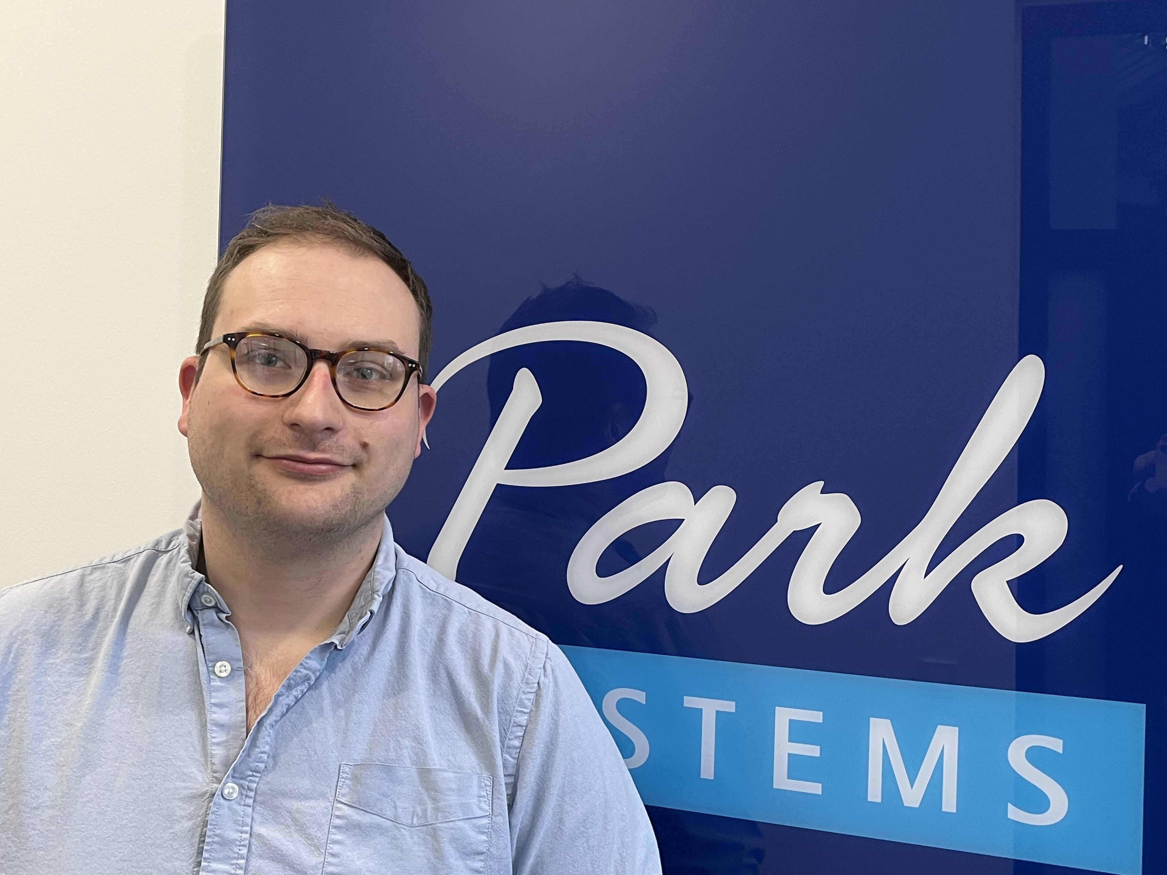
James received his PhD in Physics from the University of Nottingham in 2018, studying the morphology and optical properties of monolayers of self-assembled molecules and their heterostructures. He then went on to work as a postdoctoral researcher, also at the University of Nottingham, working on the formation of hybrid heterostructures of molecular assemblies and layered materials demonstrating both electroluminescence and selective triplet excitation. In 2020, James took up a position as a postdoctoral researcher at the Cambridge Graphene Centre, using scanning probe microscopy and optical spectroscopy to study electrostatics and optical properties of layered materials heterostructures with controlled twist angle and their scalable incorporation into integrated photonic circuits. Since January 2022, James has been a member of the Park Systems team as an applications scientist, supporting customers with interest ranging from fundamental physics to industrial scale production in the application of a diverse range of scanning probe microscopy techniques to gain insightful results.
