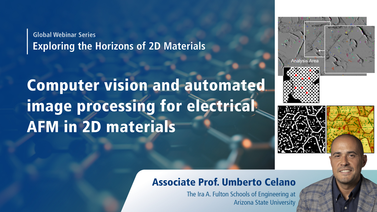
Global Webinar Series | Exploring the Horizons of 2D Materials

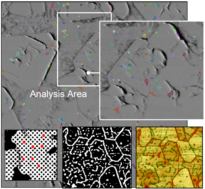
Electrical atomic force microscopies (AFMs) in their various configurations, are powerful tools for characterizing 2D materials. However, standardizing data interpretation and accelerating material screening across multiple samples remains complex largely due to analysts-induced inconsistencies and preferences that can hinder standardization. Here, we review strategies with minimal human in the loop using conductive atomic force microscopy for electrical measurements in 2D materials. We propose a strategy to integrate computer vision techniques with automated image processing to be applied in 2D materials. The aim is to minimize human intervention and gain information on some of the most relevant electrical defects such as point defects, grain boundaries, cracks, and extended defects in MoS2 relying primarily on automated systems and techniques.

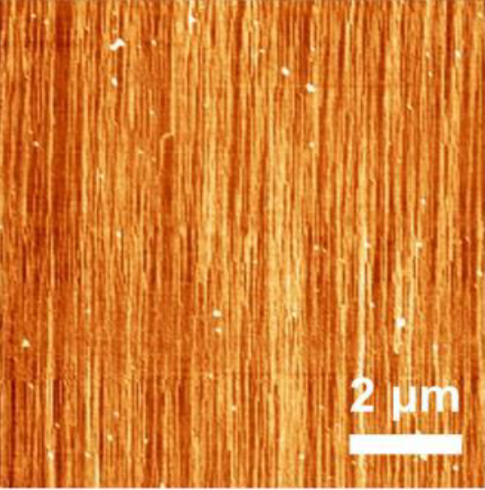
Atomic force microscope image of unidirectionally directionally controlled grown nanofibers
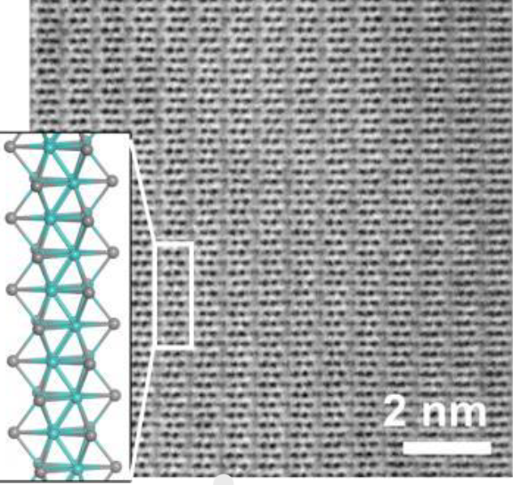
Electron microscope image and structural model of TMC atomic wire nanofibers aggregated in the same direction
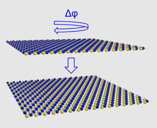
Image caption
Image caption


Umberto Celano is an Associate Professor with the Ira A. Fulton Schools of Engineering at Arizona State University. He received the B.Sc. and M.Sc. degrees in Electrical Engineering (summa cum laude) from the Sapienza University of Rome, Italy, in 2009 and 2011, respectively, and the Ph.D. degree in Physics from the University of Leuven - KU Leuven (honorable mention) in 2015. His research focuses on nanoelectronics at the interface of condensed matter physics, materials analysis, and semiconductor technology. His group studies fundamental processes underlying the operation of emerging devices, with emphasis on design and use of nanoscale analytical instruments for device reliability, failure analysis, and correlative metrology.