Advancements in 2D Materials' Characterization via ISE
In the field of 2D materials characterization, Imaging Spectroscopic Ellipsometry enable the determination of optical properties [1],[2],[3].. The data are required for a better understanding of 2D material based devices [4],[5]..
From the macroscopic point of view, ellipsometric contrast micrographs or microscopic maps of Delta and Psi can be stitched and offer a fast, non-contact, wafer-scale, atomic layer resolved imaging of 2D materials [6] on a variety of substrates. Including maps recorded at different wavelengths, a specific search for microcrystals with a dedicated number of layers or a predefined thickness was reported. Recent studies also show the possibility of imaging buried layers [7].
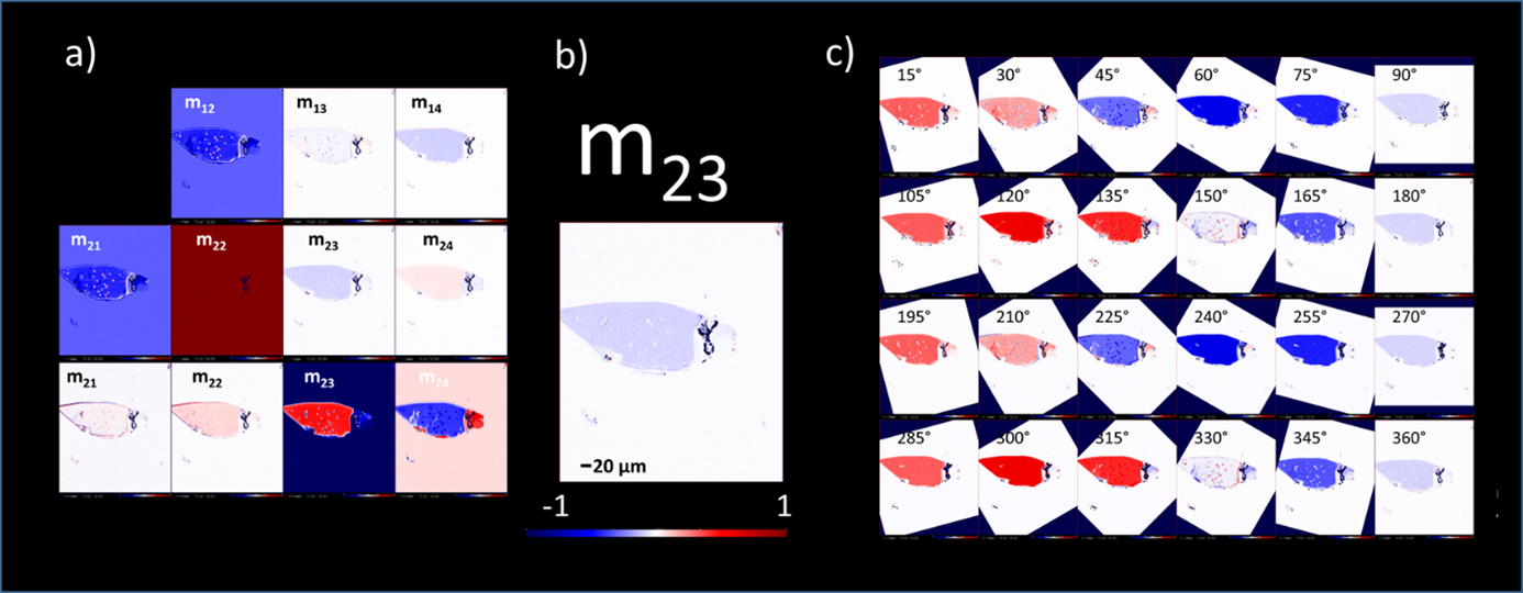
The focus of the talk will be on applications of Imaging Müller matrix ellipsometry for anisotropic microcrystals characterization. Micrographs of 11 elements of the Müller Matrix, normalized to element 1 were recorded at different wavelength and orientations for different microcrystals like Black Phosphorous or Bi2SeO5 (Fig, 1).
[1] S. Funke et al., J. Phys.: Condens. Matter 28 (2016) 385301.
[2] G.A. Ermolaev et al., Nat Commun 12 (2021), 854.
[3] P. G. Zotev et al., Laser Photonics Rev. 17 (2023), 2200957
[4] S. R. Tamalampudi et al., npj 2D Materials and Applications 8 (2024) 46.
[5] Dushaq, G. et al., Light Sci Appl 13, (2024) 92.
[6] P. Braeuninger-Weimer et al., ACS Nano 12, (2018) 8555–8563.
[7] Irina Chircă et al., 2D Mater. 11 (2024) 045001
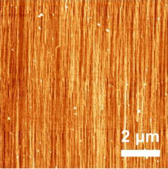
Atomic force microscope image of unidirectionally directionally controlled grown nanofibers
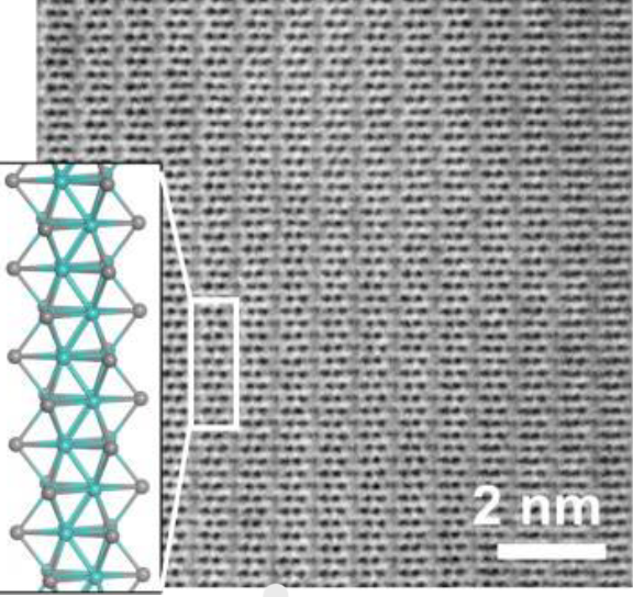
Electron microscope image and structural model of TMC atomic wire nanofibers aggregated in the same direction
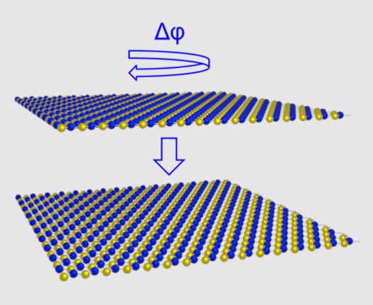
Image caption
Image caption
Ferroelectricity is observed in hexagonal boron nitride(hBN) through control of the registry of stacked layers, which we explore through both amplitude-modulated and sideband Kelvin probe force microscopy (KPFM) on the Park FX40 automatic AFM.
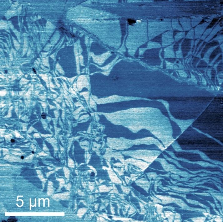
A schematic of the formation of parallel stacked bilayer hBN is shown in addition to a contact potential difference map measured using sideband KPFM.
Image caption
Image caption
Image caption


Peter received his PhD in chemistry from Kiel University in 1996. He worked for one year on a research project for the former Wella AG and then joined the Helmut Schmidt University in Hamburg, where he set up a lab for adsorption research and surface characterization, including ellipsometry. In 2006, he joined the former Nanofilm Technology GmbH as a sales manager and application specialist for imaging ellipsometry and Brewster angle microscopy. He has been a strong advocate for the benefits of imaging spectroscopic ellipsometry and has presented this technique at a number of scientific conferences and workshops. He has installed systems and trained users in more than 20 countries worldwide and spent one year in Ann Arbor, Michigan, with Accurion. He is the author/co-author of more than 30 scientific publications on a broad range of surface chemically related topics, like the intracrystalline salinization of layered crystalline silicic acids, SiO2-based nanofluids, protein immobilization for affinity separation technologies, hierarchical clustering of odor compounds, odor control, and especially the characterization of 2D materials and other applications of imaging spectroscopic ellipsometry.