Advancements in 2D Materials' Characterization via ISE

Two-dimensional (2D) materials are atomically thin crystalline layers with physical properties that dependent on the layer number. So far various families of two-dimensional materials have been realized with many materials being environmental (rather) stable and can be combined in hetero-stacks in nearly any fashion with rotational degree of freedom. Spectroscopic imaging ellipsometry is established as a powerful tool to identify and characterize such structures, to investigate interfacial properties and to study the peculiar light-matter interaction in those ultrathin systems down to the monolayer limit [1-5].
The study of two-dimensional quantum materials and the investigation of ultrathin films for quantum-technological application under in-operando conditions requires cryogenic temperatures down to the sub-Kelvin regime [6]. We combine Spectroscopic Imaging Ellipsometry (SIE), which offers the capability of an ellipsometer with the lateral resolution of a microscope with a closed-cycle cryostat with an ADR cooling stage with free beam optical access allowing SIE measurements from room-temperature down to <800mK. In this way, we explore the temperature-dependence of the local dielectric function of 2D polar gallium, a novel two-dimensional material with a superconducting phase transition at around 4.5K and strong plasmonic response and epsilon-near zero behavior [7,8]. We show a change in the local dielectric response of the material from a homogenous behavior at room temperature to a heterogenous regime at low temperatures that is interpreted as a structural phase transition in the material resulting in local changes of the dielectric response [9].
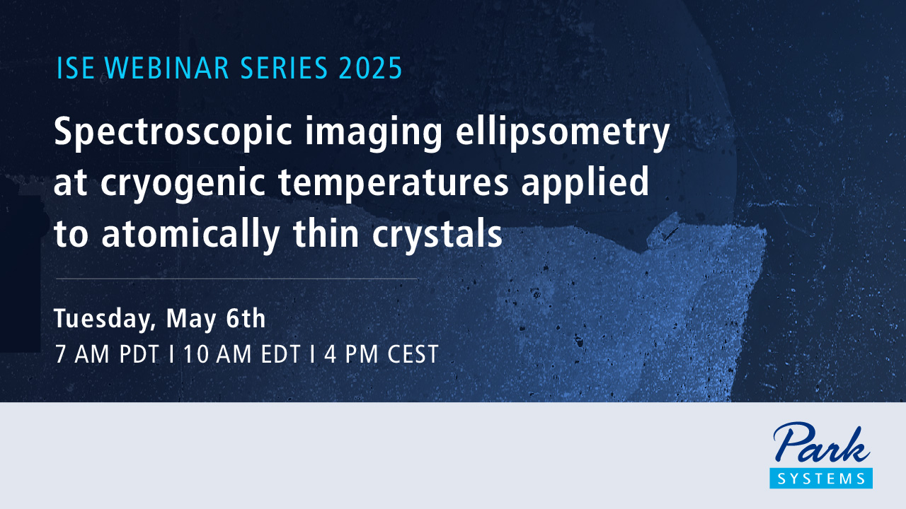
Figure 1: Optical micrograph of the low-temperature SIE set-up.
References
[1] S. Funke et al., J. Phys.: Condens. Matter 28, 385301 (2016).
[2] S. Funke et al. Applied Surface Science B 421, 435 (2017).
[3] F. Sigger et al. Apl. Phys. Lett. 121, 071102 (2022).
[4] S. Diefenbach et al. J. Phys. Chem. C, 122, 17, 9663–9670 (2018).
[5] F. Sigger et al. Apl. Phys. Lett. 121, 071102 (2022).
[6] J. Rasmus Bankwitz et al. Optics Letters 48(21), 5783-5786 (2023).
[7] K. Nisi et al., Adv. Funct. Mater. 31, 2005977 (2020).
[8] S. Rajabpour et al. Adv. Mater. 2104265 (2021).
[9] J. Henz et al. in preparation (2024).
Atomic force microscope image of unidirectionally directionally controlled grown nanofibers
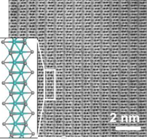
Electron microscope image and structural model of TMC atomic wire nanofibers aggregated in the same direction
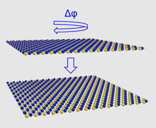
Image caption
Image caption
Ferroelectricity is observed in hexagonal boron nitride(hBN) through control of the registry of stacked layers, which we explore through both amplitude-modulated and sideband Kelvin probe force microscopy (KPFM) on the Park FX40 automatic AFM.
A schematic of the formation of parallel stacked bilayer hBN is shown in addition to a contact potential difference map measured using sideband KPFM.
Image caption
Image caption
Image caption


Ursula Wurstbauer holds a degree in Physics from the University of Regensburg in 2006, where she also received her PhD under supervision of Prof. Werner Wegscheider in 2008. After postdoc stays at Hamburg University and Columbia University in the City of New York (USA), she became a junior group leader at the Walter Schottky Institute at the Technical University of Munich in 2013 and was elected as PI of the DFG cluster of excellence “Nanosystems Initiative Munich” (NIM) and member of the cluster of excellence “e-conversion”. Since 2019, she is a full professor of Physics at university of Münster heading there the nanoelectronics group. The research of the group focuses on emergent and interaction driven phenomena of two-dimensional materials and two-dimensional charge carrier systems, related hetero-, and hybrid structures as well as interfaces. The aim is to gain a fundamental understanding of the physical properties of those systems and to learn – in a next step – to control and tailor them on purpose with the vision to achieve novel functionalities and at the same time to look for potential applications in an interdisciplinary context. Therefore, these low-dimensional systems are integrated in nano- and microscale circuitries, as well as in proof-of-concept and prototypical devices to explore their potential for opto-/electronic or energy harvesting applications and to serve as test-bed structures towards quantum technologies.