
Theoretical and hands-on sessions on ScanWaveTM (Scanning Microwave Impedance Microscopy - sMIM), the most advanced electrical AFM measurement. Topics include semiconductors, insulators, buried structures, nanowires, image sensors, and emerging materials. Join this in-person workshop for a live demonstration using PrimeNano's ScanWave on a Park NX20!
Abstract: ScanWaveTM sMIM is a near-field scanning probe microscopy technique where an AFM cantilever is used as a microwave source to measure the electrical properties of materials at the nanoscale. Microwave signals are sent through an AFM cantilever and the reflected signal is collected. The reflected microwave signal is a measure of the impedance of the sample underneath the AFM tip. sMIM provides images of the variations in the local capacitance and conductance with nanoscale resolution making it an excellent method for characterizing a wide range of materials such as semiconductors, insulators, 1D/2D, ferroelectric materials and more.
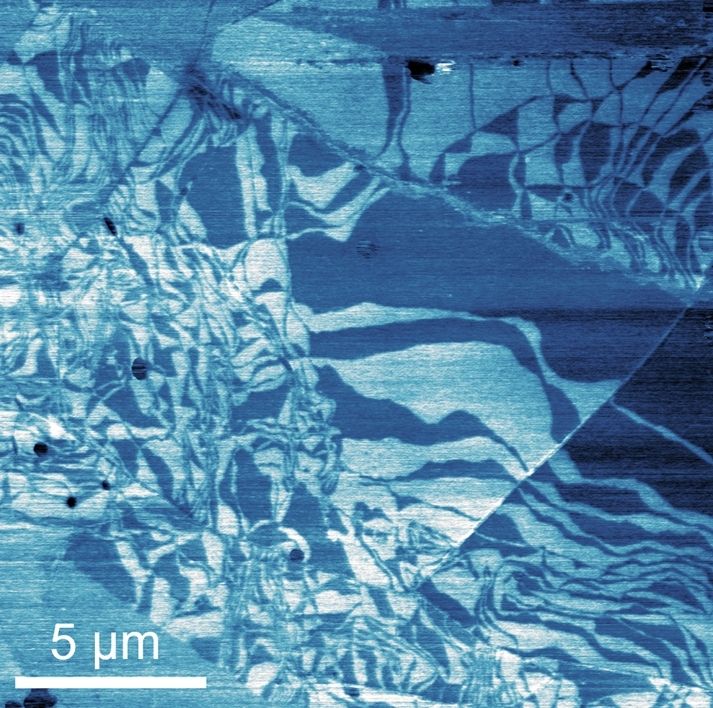
Ferroelectricity is observed in hexagonal boron nitride(hBN) through control of the registry of stacked layers, which we explore through both amplitude-modulated and sideband Kelvin probe force microscopy (KPFM) on the Park FX40 automatic AFM.
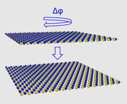
A schematic of the formation of parallel stacked bilayer hBN is shown in addition to a contact potential difference map measured using sideband KPFM.
Image caption
Image caption
Image caption